WAFER PROCESS TECHNOLOGIES
The facility allows 4" and 6" wafer processing. The following lists
available process technologies at the facility.
 Lithography
- <1um resolution
- EVG 620 Precision Alignment System & Bond Aligner for 4" and 6"
- Karl Suss MA 56 Aligner
Mask Plate Making
Wafer Bonding
-
EVG 501 Universal Bonder 4" and 6"
-
Silicon to glass anodic bonding
-
Eutectic bonding
-
Thermocompression bonding
-
Fusion Bonding
Deep Reactive Ion Etching (DRIE)
- STS Multiplex ASE HRM System for 4" and 6" wafers, upgradeable to 8"
Plasma Enhanced Chemical Vapor Deposion (PECVD)
- STS Multiplex CVD System for 4" and 6" wafers, upgradeable to 8"
-
Silicon Dioxide
-
Stress free silicon nitride
-
Amorphous silicon
-
PhosphoSilicate Glass (PSG)
-
BoroPhosphoSilicate Glass (BPSG)
-
Reactive Ion Etching (RIE) capability
Reactive Ion Etching (RIE)
- STS Multiplex RIE System for 4" and 6" wafers, upgradeable to 8"
-
Silicon Dioxide
-
Silicon nitride
-
Aluminum
-
BCB
-
Polyimide
-
Non-plasma silicon etching based on Xenon Difluoride (XeF2) gas
Dry / Wet Oxidation
-
RCA cleaning prior to high-temperature treatment
-
Atmospheric thermal dry oxidation
-
Atmospheric thermal wet oxidation
-
High temperature drive-in under inert atmosphere
-
5 furnaces, THERMCO
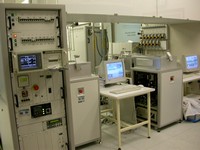
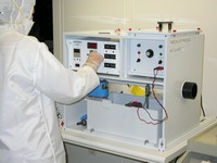
Diffusion
-
Boron diffusion using BBr3 and B2H6 gases
-
Phosphorus diffusion using POCl3 gas
-
26 furnaces, THERMCO
Etching
-
Silicon dioxide etching with BHF solution
-
Silicon nitride etching
-
Anisotropic silicon etching using KOH, TMAH, and EDP
-
Isotropic silicon etching using HNA
-
Electrochemical etching using KOH and TMAH solutions
-
Metal etching: Al, Cu, Ti, Ni, Cr, Au
-
Resist stripping in organic solvents
Plasma Etching
Electroplating (FIBRoplate process, uniformly on 4" & 6"
wafers)
-
Nickel electroplating
-
Copper electropating
-
Gold electroplating

Nickel electroplated comb fingers.


Nickel electroplated comb fingers with 4um spacing.
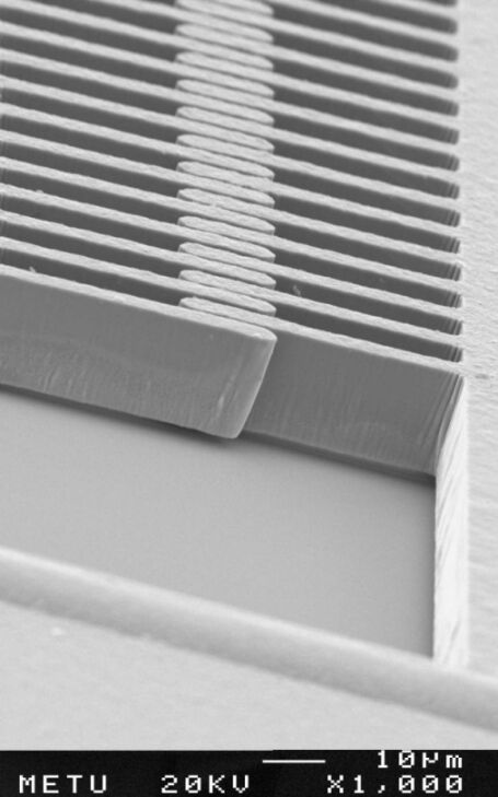
High-aspect ratio nickel electroplated comb fingers with 4um-spacing.
SU-8 molding (Under development)

SU-8 patterns. Feature size: 5-20 um, height: 35-40 um.
Evaporation and Sputterring (Al, Au, Au/As, Ni, Cr, Ni-Cr, Cu,
Ti)
-
VARIAN 3119 e-gun source system & BALZERS BAS 450 PM planar magnetron
sputtering system
-
BALZERS BAS 450 PM planar magnetron sputtering system
Passivation
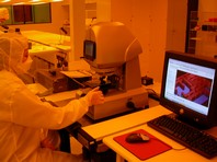
Metrology
-
Veeco Dektak 8 Profiler
-
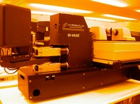
Veeco Wyko NT 1100 Profiler
-
FTIR-210 IR-VASE Elipsometer
-
Nanospec/AFT Computerized Film Thickness Measurement System
-
Magnetron Model M-700 Four Point Probe System
-
JEOL Scanning Electron Microscope (SEM)
-
Karll Suss PM5 Manual Probe Station with Laser Cutter
-
Airborn particle scanner
-
Optical inspection x100
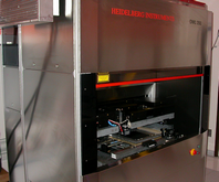
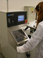
Wafer Dicing
-
DISCO DAD 3350
-
DISCO DAD 321
-
Silicon, glass, silicon-to-glass bonded and GaAs substrates
-
Dicing
Request Form
Wire-Bonding
-
Kluicke & Soffa Manual Gold Wire-Bonder
Back-lapping (SPEEDFAM)